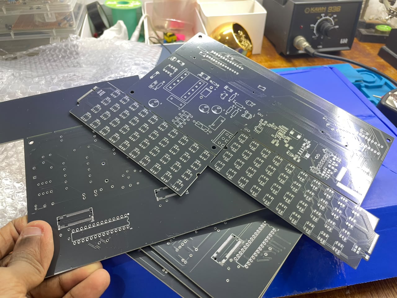
PCB Layout Checklist for Small Control Boards
PCB Design

PCB Layout Checklist for Small Control Boards

A practical pre-fabrication checklist for headers, mounting holes, power paths, and labels.

Cyfersnare Lab / 2026-06-14 / 5 min read

Small boards fail in boring ways: unlabeled connectors, awkward mounting holes, unclear polarity, or power paths that are too thin.

Before fabrication, review connector direction, enclosure fit, mounting clearance, test points, silkscreen labels, and expected current.

The best board file is one that still makes sense when you return to it months later.

Gallery placeholder

Future admin-managed galleries can attach process photos, screenshots, board renders, and finished build images here.

Related posts

More notes from the build log.

Build Logs

Build Logs

Test XSS

<img src="x" onerror="console.log('XSS-TEST-EXCERPT')"/>

2026-06-254 min read
Read More
fsaffasfa
3D Printing

fsaffasfa

Tags hello

ffasf4 min read
Read More

Shopping Cart

0

Your cart is empty

Add prototype boards, accessory kits, or custom printed parts from the catalog.

Estimated Total
රු 0.00